Applied electricity
Course notes of Applied electricity by Lecturer 林冠中.
Course information
- Lecturer: 林冠中 (calculus365(at)yahoo.com.tw)
- Time: Fri. ABCD
- Location: EE1-201 Lab
- Office hour (please make a reservation by email):
- Mon. 5 pm
- Tue. evening
- Fri. after class
TL;DR
- SI units for electrical circuits:
- time(t): second
- current(i): Ampere
- voltage(v): Volt
- resistance(r): Ohm
-
power(p): Watt
- Directionality matters. Negative sign = opposite direction
- Minus to plus: voltage gain; plus to minus voltage drop
- Ohm's Law: V = IR
- Kirchhoff's circuit laws
- KCL : \(Σi_{in} = Σi_{out}\) (on a node)
- KVL : \(ΣV_{drop} = ΣV_{supply}\) (around a loop)
- Power: \(P = IV\)
Current
- Flow of positive charge versus time: \(i(t) = \frac{dq}{dt}\)
- 1 Ampere = 1 Coulomb per second
Voltage
- Change in energy (in Joules) from moving 1 Coulomb of charge
- 1 Volt = 1 Joule change per Coulomb: \(V = \frac{Q}{C}\)
- Change in electrical potential (\(φA - φB\))
- Ground: V = 0 (manually set)
- \(V_{ab} = V_{a} - V_{b}\)
- Power supplier (source): pointing from minus (-) to plus (+)
- Power receiver (load): pointing from plus (+) to minus (-)
Dependent sources
Find where the depending parameter is and note the units. Wikipedia
Power balance
Rule of thumb: supply = load. Beware directionality of both current and voltage across a device.
Resistive circuits, Nodal and mesh analysis
- Conductance G = 1/R, Unit: Siemens (S)
- Short circuit: V = 0, R = 0
- Open circuit: I = 0, G = 0
- Passive component: R >= 0
- Parallel circuit: same voltage
- Serial circuit: same current
Nodal analysis
- Use Kirchhoff's current laws (current in = current out)
- Grounding (set V = 0) on one of the node.
- Super-node (Voltage source): direct voltage difference between nodes, reducing the need to find currents
Loop (mesh) analysis
- Use Kirchhoff's voltage laws (voltage supplied = voltage consumed)
- Note that currents add up in common sides of the loops.
- Super-mesh (Current source): direct current inference in the loop.
Series / parallel circuits
- Serial: one common point. \(R_s = R_1 + R_2\)
- Parallel: two common points. \(R_p = \frac{R_1R_2}{R_1 + R_2}\)
- Analysis: combining resistors bottom-up.
- Voltage divider: series resistors
- Current divider: parallel resistors
Resistor tolerance
- Last colored ring on the resistor.
- Need to design some room for the components according to the tolerance (min and max values)
Y-Δ transformation
https://en.wikipedia.org/wiki/Y-%CE%94_transform
- Δ -> Y: denominator = sum of the three; numerator = product of the twos next to the node
- Y -> Δ: denominator = the opposite one; numerator = sum of products of two
- Electric bridge balance: products of the opposite sides are the same
- central current = 0 => equivalent to open circuit
Question
What is the difference between node and loop analysis?
The principle of superposition
- Effects of multiple sources could be added (superposition) individually.
- Remove voltage source = short circuit
- Remove current source = open circuit
Thevenin and Norton equivalent circuits
- Simplifying circuit in a black box from the principle of superposition
- Find equivalent resistance (\(R_{TH}\)) after source removal.
- Find equivalent open circuit voltage (source) for Thevenin's theorem
- Or, find equivalent short circuit current (source) for Norton's theorem
For dependent sources
- Pure dependent sources cannot self-start: \(V_{TH}\) = 0
- Finding \(R_{TH}\) requires a probe source: \(R_{TH} = {V_p}/{I_p}\)
- I_p : short circuit current with a probe source
- Like one would do in a an circuit experiment
Maximum power transfer
When \(R_{Load} = R_{TH}\), the power is maximum $P = V{TH}^2 / (4R) $
Norton's theorem
- \(R_{TH}\) the same as Thevenin
- \(I_{SC}\) : short circuit current instead of open circuit voltage
- \(I_{SC} = V_{OC} / R_{TH}\)
Capacitors and Capacitance
- \(i = C \frac{dV}{dt}\)
- Smooth voltage change
- At t=0 and uncharged: short-circuit
- DC steady-state: open-circuit
- Energy stored: \(0.5CV^2\)
- Series / Parallel: opposite to resistors
Inductors and Inductance
- \(v = L \frac{di}{dt}\)
- Smooth current change
- At t=0 and no mag. flux: open-circuit
- DC steady-state: short-circuit
- Energy stored: \(0.5Li^2\)
- Series / Parallel: the same as resistors
AC steady-state analysis
- Periodic signal: \(x(t) = x(t + nT)\)
- Sinusoidal waveform: \(x(t) = Acos(\omega t + \phi)\)
- \(\omega = 2\pi f\)
- \(f = 1/T\)
- \(2\pi\) rad = 360 degrees
RMS (Root mean square), effective value
- Peak = \(\sqrt{2}\) RMS value for sinusoidal current and voltage.
Phase lead / lag
- Leads by 45 degrees: \(x(t) = Acos(\omega t + 45^o)\)
- Lags by 45 degrees: \(x(t) = Acos(\omega t - 45^o)\)
- Pure capacitor + AC circuit: current leads voltage by 90 degrees
- Pure inductor + AC circuit: current lags voltage by 90 degrees
Complex algebra
- Euler's formula: \(e^{j\theta} = cos(\theta) + sin(\theta)\)
- Frequency term (\(e^{j\omega t}\)) is usually omitted in favor of angle notation.
- Multiplication: angle addition; division: angle subtraction for waveforms of the same freq.
Impedance
- Generalization to resistance in the complex domain
- The same way in calculations as that in the case of resistance
- Admittance: Generalization to conductance (reciprocal of impedance)
- Inductor: \(Z_{L} = j\omega L\)
- Capacitor: \(Z_{C} = 1/(j\omega C)\)
- Impedance is frequency-dependent. Higher freq: higher impedance from inductors; lower freq: higher impedance from capacitors
Filter
- Proved from impedance analysis
- Frequency response: transfer function = gain function
- Low pass filter: the RC circuit
- Bode plot: x: input frequency (log scale), y: response (amplitude)
RC, RL, and RLC circuits
- First, convert it to the equivalent circuit (Thevenin) for further analysis
- Time constants may be different in charging / discharging due to different circuits
RC transients
- Voltage is continuous, while current is not.
- For uncharged capacitor, initial voltage across the capacitor is zero (i.e. short circuit)
- when charging, it approaches applied voltage. The steady-state is open circuit.
- Discharging: positive voltage and negative current.
- Time scale \(\tau_{C} = RC\)
- Charging transient: \(v_{C} = E - i_{C}R\), \(i_{C} = \frac{E}{R}e^{-t/\tau_{C}}\)
- Discharging transient: \(v_{C} = V_0e^{-t/\tau_{C}}\), \(i_{C} = -v_{C}/ R\)
- \(t/\tau_{C} > 5\): > 99% completed charging / discharging
RL transient
- Current is continuous, while voltage is not.
- For uncharged inductor, initial current is zero (open circuit); then approaches terminal current upon charging. The steady-state is short circuit.
- Discharging: positive current and negative voltage (Lenz's law).
- Time scale \(\tau_{L} = L/R\)
- Charging transient: \(v_{L} = Ee^{-t/\tau_{L}}\), \(i_{L} = (E - v_{L}) / R\)
- Discharging transient: \(v_{L} = -I_0Re^{-t/\tau_{L}}\), \(i_{L} = I_0e^{-t/\tau_{L}}\)
RLC transients
- Solving series RLC circuit by KVL: \(V_R + V_L + V_C = E\)
- \(\frac{d^2I}{dt^2} + \frac{R}{L}\frac{dI}{dt} + \frac{I}{LC} = 0\), due to E is constant (DC)
- Let \(I = e^{\lambda t}\), \(\lambda = \frac{-R}{2L} \plusmn \sqrt{(\frac{R}{2L})^2 - \frac{1}{LC}}\)
- Resonant frequency: \(\omega_0^2 = \frac{1}{LC}\)
- Solving parallel RLC circuit by KCL: the same resonant frequency: \(\omega_0^2 = \frac{1}{LC}\)
Damping
- Overdamping: \((\frac{R}{2L})^2 - \frac{1}{LC} > 0\)
- Critical damping: \((\frac{R}{2L})^2 - \frac{1}{LC} = 0\) (decaying faster than overdamping)
- Underdamping: \((\frac{R}{2L})^2 - \frac{1}{LC} < 0\), oscillation (+)
Quality factor

- At resonance: \(Z_{C}\) and \(Z_{L}\) cancel each other out
- \(Q = f_{r} / BW\)
- BW: Bandwidth
- Series RLC: \(Q = \frac{1}{R}\sqrt{\frac{L}{C}}\)
- Parallel RLC: \(Q = \frac{R}{1}\sqrt{\frac{C}{L}}\)
Steady state power analysis
- Note and specify the difference between peak values (\(I_{M}\), \(V_{M}\)) and the effective (RMS) values.
- $ p = \frac{VM IM}{2}(cos(\thetav - \thetai) + cos(2\omega t + \thetav + \thetai))$
- Twice the frequency: \(2\omega t\) compared to current and voltage
- Average power: $VM IM cos(\thetav - \thetai)/2 = V{rms} I cos(\thetav - \thetai) = P_{app} \cdot pf $
- Apparent power: \(P_{app} = V_M I_M / 2 = V_{rms} I_{rms}\)
- Power factor: \(pf = cos(\theta_v - \theta_i)\). The phase difference between voltage and current
- Purely resistive: \(p = V_M I_M / 2 = V_{rms} I_{rms}\). pf = 1
- Purely capacitive / inductive: \(p = pf = 0\). Does not absorb power on average.
- For average power, one could calculate the resistive part only.
Maximum power transfer
When \(Z_{L} = Z_{TH}^*\) , Im(ΣZ)= 0,
\(P_{L,max} = 0.5 * \frac{\lvert V_{OC} \rvert\ ^2 }{4 R_{TH}}\) (Since \(P = 0.5 V_{M}I_{M}\))
Power factor and complex power
- \(p = V_M I_M cos(\theta_v - \theta_i)/2 = P_{app} \cdot pf\). Unit:VA
- Phase difference = 0 (purely resistive), pf = 1
- Phase difference = -90 (purely capacitive) or 90 (purely inductive), pf = 0
Active power vs reactive power
\(S = P_{app} cos(\theta_v - \theta_i) + jP_{app} * sin(\theta_v - \theta_i)\)
* Former: active power (P); latter: reactive power (Q)
* \(\lvert S \rvert = \sqrt{P^2 + Q^2} = P_{app} = V_{rms} I_{rms}\)
* \(P = \lvert S \rvert \cdot pf\)
* For capacitive circuit: Q < 0; inductive circuit: Q > 0
Safety considerations
- 100 mA to the heart: Ventricular tachycardia and could be fatal
- Grounding: increase safety by shunt the current away from the user in case of fault
- Ground fault interrupter(GFI):

- No fault: In current = out current, do nothing
- Fault: If current is not the same as out, it induces current in the sensing coil and breaks the circuit.
- Accidental grounding: new path for currents, new hazard.
Magnetically coupled circuits
Mutual inductance
- Open circuit \(v_2 = L_{21}\frac{di_1}{dt}\)
- Two current sources: self inductance plus mutual inductance
- \(v_1 = L_1\frac{di_1}{dt} + L_{12}\frac{di_2}{dt}\)
- \(v_2 = L_{21}\frac{di_1}{dt} + L_{2}\frac{di_2}{dt}\)
- Beware the dot (current direction of the input and output): turn them into standard circuit
- The linear model states \(L_{21} = L_{12} = M\)
- Mutual inductance in series inductors: \(L_{eq} = L_1 + L_2 \pm 2M\)
- Mutual inductance in parallel inductors: \(L_{eq} = \frac{L_1L_2 - M^2}{L_1 + L_2 \mp 2M}\)
Energy analysis
- \(w = 0.5L_1I_1^2 + 0.5L_2I_2^2 \pm MI_1I_2\)
- \(M \le \sqrt{L_1L_2}\), the geometric mean of L1 and L2
- \(k = \frac{M}{\sqrt{L_1L_2}}\), coupling coefficient (0 to 1)
Transformers
- Iron core, air core, composite core
- Ideal transformers: no energy loss (Pin = Pout)
- \(\frac{V_1}{V_2} = \frac{N_1}{N_2}\)
- \(\frac{i_1}{i_2} = \frac{N_2}{N_1}\)
-
\(\frac{Z_1}{Z_2} = (\frac{N_1}{N_2})^2\)
-
Analysis of simple transformer circuits (PhD qualification exam)
- Application: AC -> transformer -> rectifier -> filter -> regulator -> DC
- Practical transformers
- Leakage of magnetic flux
- Winding resistance: copper loss
- Core loss: eddy current, hysteresis
- efficiency: \(\eta = \frac{P_{out}}{P_{in}}\)
Frequency response
- Resistive circuit: freq-independent \(|Z_R|\) = const, θ = 0
- Inductive \(|Z_L|\varpropto f\), θ = 90
- Capacitive \(|Z_C|\varpropto 1/f\), θ = -90
Series RLC
\(Z_{eq} = R + j\omega L + \frac{1}{j\omega C}\)
\(|Z_{eq}| = \frac{\sqrt{(\omega RC)^2 + (1-\omega^2LC)^2}}{\omega C}\)
- Minimal \(|Z_{eq}|\) when \(\omega = \omega_0 = \frac{1}{\sqrt{LC}}\) (resonant frequency) and \(Im(Z_{eq}) = 0\)
Bode plot
- x-axis: freq (log(f) )
- y-axis: magnitude (20*log(M), in dB) / phase (in degrees)
- dB is for power amplification / attenuation
- dBm = \(10log\frac{p}{1mW}\)
Multistage system
- Amplitude: product of all systems
- dB: sum of all dB gains
Network transfer function
Thevenin equivalence theorem for finding the gain.
Bandwidth
Dependent on reactive elements (usually RC circuits, inductors are more difficult to handle)
Cutoff frequency: -3dB (0.707x) voltage magnitude (half power)
Quality factor and effective bandwidth
Series RLC: \(Q = \frac{\omega_0 L}{R} = \frac{1}{R}\sqrt{\frac{L}{C}}\)
Bandwidth (BW) = \(\omega_0\) / Q = \(\omega_{hi} - \omega_{lo}\)
\(\omega_{hi} \omega_{lo} = \omega_0^2\)
Poles and Zeros
Let \(s = j\omega\) (Laplace transform)
For series RLC:
\(Z_{eq} = R + sL + \frac{1}{sC} = \frac{s^2LC + sRC + 1}{sC}\)
\(H(s) = K_0 \frac{(s-z_1)(s-z_2)...}{(s-p_1)(s-p_2)...}\)
- \(K_0\) : DC term
- zeros: H(s) = 0
- poles: H(s) diverges
Filters
- Low-pass <-> high pass by an RC circuit
- Band-pass <-> band reject (notch filter) by an RLC circuit or a combination of a low-pass and a high-pass filter
OP-Amp
Ideal OP-Amp

- Infinite open-loop gain G = \(v_{out} / v_{in}\)
- Infinite input impedance \(R_{in}\), thus zero input current
- Zero input offset voltage
- Infinite output voltage range, not clipped by supplied voltage
- Infinite bandwidth with zero phase shift and infinite slew rate
- Zero \(R_{out}\), output impedance
- Zero noise
- Infinite common-mode rejection ratio (CMRR)
- Infinite power supply rejection ratio.
Circuit analysis in Ideal OP-Amp
- \(V_{-} \approx V_{+}\)
- \(i_{-+} \approx 0\)
- Make sure \(V_{out}\) is in the range of supplied voltages.
The rest is Ohm's law and circuit analysis.
More OP-Amp circuits
Multiple input voltages
Principle of superposition. One voltage source at a time.
With energy-storing devices
- Differentiator
- Integrator
- Antoniou Inductance Simulation Circuit
\(L = C_4 R_1 R_3 R_5 / R_2\)
Semiconductors
Materials
- Group IV: Si, Ge
- Group III + V: GaN, GaAs(P)
Why semi-conductivity
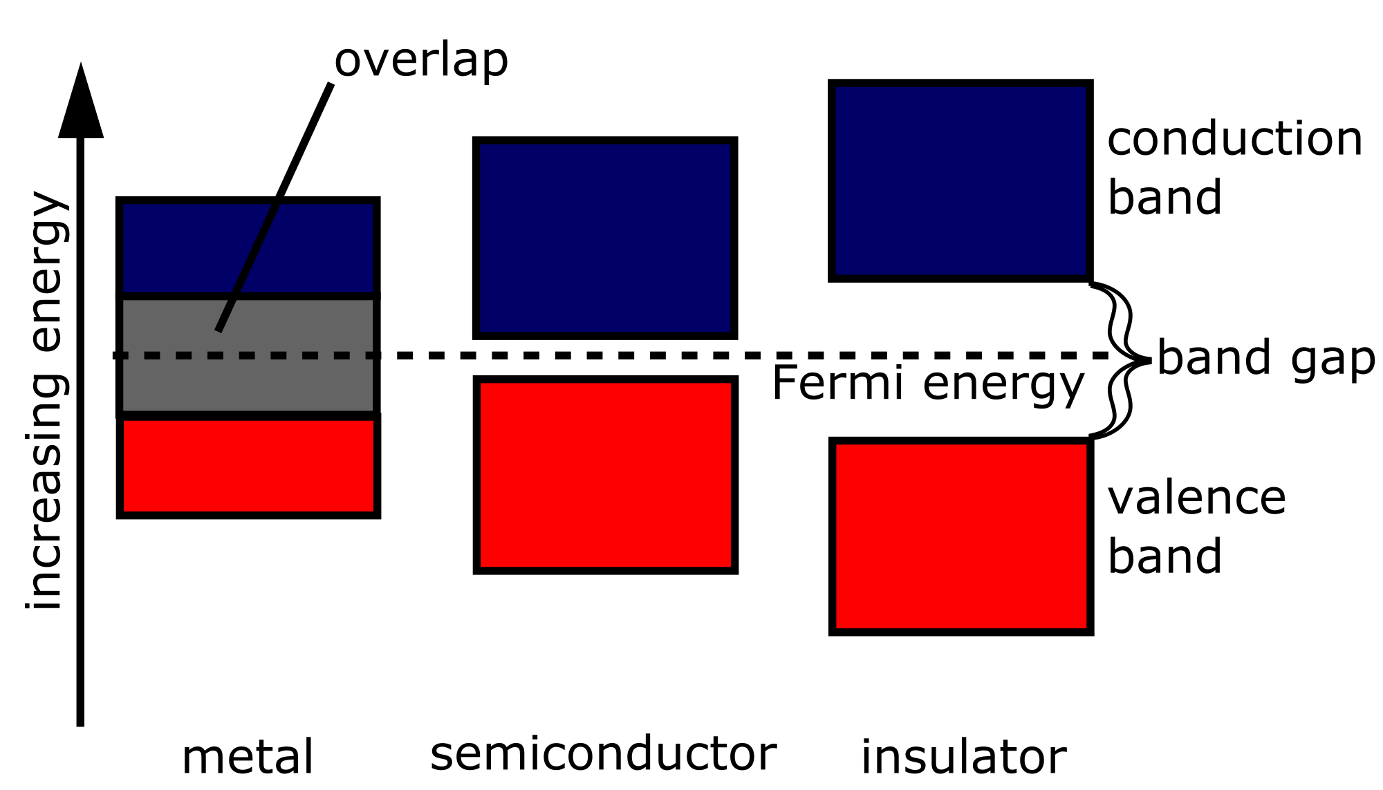
- Band gap energy difference \(E_{g}\) = \(E_{c}\) - \(E_{v}\)
- Insulators: > 5 eV
- Semiconductors: smaller gap, a small amount of electrons escape from valence band to the conduction band
- Conductors (metal, graphite): overlap (no gap)
- Direct (III+V) vs indirect (IV) band gaps
- Direct: could emit photons (LED, photo detector)
- Indirect: emit a phonon in the crystal
- The tetrahedral covalent bond crystalline structure for extrinsic (doped) semiconductors
Carriers
- Electrons (e-) in the conduction band as well as the vacancies in the valence band (holes, h+)
- For intrinsic semiconductors, motility factor \(\mu\): GaN (GaAs) >Ge > Si, parallel with conductivity
- Enriched by doping (increase both \(\mu\) and conductivity): making extrinsic semiconductors
- Doping group V elements (donor impurities): electrons are major carriers (N-type)
- Doping group III elements (acceptor impurities): holes are major carriers (P-type)
- N-type semiconductors have higher \(\mu\) than P-type since electrons have lower effective mass than holes. Thus, N-type is better for high-freq applications. But P-type has dual role, being both resistors and semiconductor switches.
P-N junctions and diodes
Depletion zone
- Diffusion of major carriers generate an electric field across the boundary
- A zone with little carriers, high resistance
- Process a barrier voltage
Applying voltage
- Forward bias: shrinking depletion zone, high conductivity
- Reverse bias: widening depletion zone, very low conductivity (essentially open circuit until breakdown)
Shockley equation
\(I_{D} = I_{S} (exp(V/V_{T}) - 1)\),
where \(V_{T} = \frac{kT}{q} = \frac{RT}{F} = 26mV\) (Thermal voltage)
- Forward bias: shrinking depletion zone
- Reverse bias: widening depletion zone, very low conductivity (essentially open circuit until breakdown)
Three representations of diodes
Assuming there are internal resistance (\(R_D\)), threshold voltage (\(V_D\)).
* For \(V \le V_D\), open circuit.
* For \(V \geq V_D\), equivalent to a reverse voltage source of \(V_D\).
- Ideal diodes: \(R_D = 0\), \(V_D = 0\). Forward bias: short circuit. Reverse bias: open circuit.
- With barrier voltage (Si = 0.6~0.7 V; Ge = 0.2~0.3V): \(R_D = 0\), \(V_D \neq 0\).
- Practical diodes: \(R_D \neq 0\), \(V_D \neq 0\)
Diode circuits
Transform diodes into equivalent components.
Rectifiers
Only half wave rectification was covered.

Limiters (cutters)
Filters
When the load resistance is infinite (open circuit): peak detector
When the load resistance is finite:
The more discharging time scale ( \(\tau = RC\) ), the less ripple voltage. ( \(V_r \approx \frac{V_p}{fCR}\) when \(V_r \ll V_p\) )
Voltage regulator using Zener diodes
- First unplug the Zener diode and solve the voltage across it.
- Normally operates in reverse bias. ( \(V_{Z}\) = 4-6 V )
- When applied voltage > \(V_{Z}\): Acts as a voltage source of \(V_{Z}\). Open circuit otherwise.
- When in forward bias: similar to regular diodes ( \(V_{Z}\) = 0.7 V )
- When breakdown \(V_{Z}\) is independent of loading resistance.
BJT
Bipolar junction transistor on Wikipedia
Current control devices.
Symbol
NPN BJT (more common)
.svg)
PNP BJT (less common nowadays)
_jP.svg)
- B: Base
- C: Collector
- E: Emitter
Math
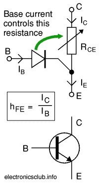
- \(I_C = \beta I_B\), \(\beta \gg 1\) (typically 80-180)
- \(I_E = I_C + I_B = (1 + \beta) I_B\)
- BArrier voltage: \(V_{BE} \approx 0.7\) Volt for Si BJT. 1.1 V for GaN BJT.
- \(I_{Csat} \approx \frac{V_{CC}-0.2}{R_C + R_E}\)
- \(\beta I_B = I_C \leq I_{Csat}\)
The rest is regular circuit analysis (KCL, KVL).
One could use the fact that \(I_B\) is very small (\(\mu A\)) compared to other currents (\(mA\)).
MOSFET
Voltage control devices.
- Gate voltage \(V_{GS}\) is greater than threshold (\(V_t\)): low resistance, (ideally) short circuit.
- Otherwise, high resistance, (ideally) open circuit.