Applied electricity
Course notes of Applied electricity by Lecturer 林冠中.
Course information
- Lecturer: 林冠中 (calculus365(at)yahoo.com.tw)
- Time: Fri. ABCD
- Location: EE1-201 Lab
- Office hour (please make a reservation by email):
- Mon. 5 pm
- Tue. evening
- Fri. after class
TL;DR
SI units for electrical circuits:
Directionality matters. Negative sign = opposite direction
- Minus to plus: voltage gain; plus to minus voltage drop
Ohm’s Law: V = IR
- KCL : $Σi_{in} = Σi_{out}$ (on a node)
- KVL : $ΣV_{drop} = ΣV_{supply}$ (around a loop)
Power: $P = IV$
Current
- Flow of positive charge versus time: $i(t) = \frac{dq}{dt}$
- 1 Ampere = 1 Coulomb per second
Voltage
- Change in energy (in Joules) from moving 1 Coulomb of charge
- 1 Volt = 1 Joule change per Coulomb: $V = \frac{Q}{C}$
- Change in electrical potential ($φA - φB$)
- Ground: V = 0 (manually set)
- $V_{ab} = V_{a} - V_{b}$
- Power supplier (source): pointing from minus (-) to plus (+)
- Power receiver (load): pointing from plus (+) to minus (-)
Dependent sources
Find where the depending parameter is and note the units. Wikipedia
Power balance
Rule of thumb: supply = load. Beware directionality of both current and voltage across a device.
Resistive circuits, Nodal and mesh analysis
- Conductance G = 1/R, Unit: Siemens (S)
- Short circuit: V = 0, R = 0
- Open circuit: I = 0, G = 0
- Passive component: R >= 0
- Parallel circuit: same voltage
- Serial circuit: same current
Nodal analysis
- Use Kirchhoff’s current laws (current in = current out)
- Grounding (set V = 0) on one of the node.
- Super-node (Voltage source): direct voltage difference between nodes, reducing the need to find currents
Loop (mesh) analysis
- Use Kirchhoff’s voltage laws (voltage supplied = voltage consumed)
- Note that currents add up in common sides of the loops.
- Super-mesh (Current source): direct current inference in the loop.
Series / parallel circuits
- Serial: one common point. $R_s = R_1 + R_2$
- Parallel: two common points. $R_p = \frac{R_1R_2}{R_1 + R_2}$
- Analysis: combining resistors bottom-up.
- Voltage divider: series resistors
- Current divider: parallel resistors
Resistor tolerance
- Last colored ring on the resistor.
- Need to design some room for the components according to the tolerance (min and max values)
Y-Δ transformation
https://en.wikipedia.org/wiki/Y-%CE%94_transform
- Δ -> Y: denominator = sum of the three; numerator = product of the twos next to the node
- Y -> Δ: denominator = the opposite one; numerator = sum of products of two
- Electric bridge balance: products of the opposite sides are the same
- central current = 0 => equivalent to open circuit
Question
What is the difference between node and loop analysis?
The principle of superposition
- Effects of multiple sources could be added (superposition) individually.
- Remove voltage source = short circuit
- Remove current source = open circuit
Thevenin and Norton equivalent circuits
- Simplifying circuit in a black box from the principle of superposition
- Find equivalent resistance ($R_{TH}$) after source removal.
- Find equivalent open circuit voltage (source) for Thevenin’s theorem
- Or, find equivalent short circuit current (source) for Norton’s theorem
For dependent sources
- Pure dependent sources cannot self-start: $V_{TH}$ = 0
- Finding $R_{TH}$ requires a probe source: $R_{TH} = {V_p}/{I_p}$
- I_p : short circuit current with a probe source
- Like one would do in a an circuit experiment
Maximum power transfer
When $R_{Load} = R_{TH}$, the power is maximum $P = V_{TH}^2 / (4R_{TH}) $
Norton’s theorem
- $R_{TH}$ the same as Thevenin
- $I_{SC}$ : short circuit current instead of open circuit voltage
- $I_{SC} = V_{OC} / R_{TH}$
Capacitors and Capacitance
- $i = C \frac{dV}{dt}$
- Smooth voltage change
- At t=0 and uncharged: short-circuit
- DC steady-state: open-circuit
- Energy stored: $0.5CV^2$
- Series / Parallel: opposite to resistors
Inductors and Inductance
- $v = L \frac{di}{dt}$
- Smooth current change
- At t=0 and no mag. flux: open-circuit
- DC steady-state: short-circuit
- Energy stored: $0.5Li^2$
- Series / Parallel: the same as resistors
AC steady-state analysis
- Periodic signal: $x(t) = x(t + nT)$
- Sinusoidal waveform: $x(t) = Acos(\omega t + \phi)$
- $\omega = 2\pi f$
- $f = 1/T$
- $2\pi$ rad = 360 degrees
RMS (Root mean square), effective value
- Peak = $\sqrt{2}$ RMS value for sinusoidal current and voltage.
Phase lead / lag
- Leads by 45 degrees: $x(t) = Acos(\omega t + 45^o)$
- Lags by 45 degrees: $x(t) = Acos(\omega t - 45^o)$
- Pure capacitor + AC circuit: current leads voltage by 90 degrees
- Pure inductor + AC circuit: current lags voltage by 90 degrees
Complex algebra
- Euler’s formula: $e^{j\theta} = cos(\theta) + sin(\theta)$
- Frequency term ($e^{j\omega t}$) is usually omitted in favor of angle notation.
- Multiplication: angle addition; division: angle subtraction for waveforms of the same freq.
Impedance
- Generalization to resistance in the complex domain
- The same way in calculations as that in the case of resistance
- Admittance: Generalization to conductance (reciprocal of impedance)
- Inductor: $Z_{L} = j\omega L$
- Capacitor: $Z_{C} = 1/(j\omega C)$
- Impedance is frequency-dependent. Higher freq: higher impedance from inductors; lower freq: higher impedance from capacitors
Filter
- Proved from impedance analysis
- Frequency response: transfer function = gain function
- Low pass filter: the RC circuit
- Bode plot: x: input frequency (log scale), y: response (amplitude)
RC, RL, and RLC circuits
- First, convert it to the equivalent circuit (Thevenin) for further analysis
- Time constants may be different in charging / discharging due to different circuits
RC transients
- Voltage is continuous, while current is not.
- For uncharged capacitor, initial voltage across the capacitor is zero (i.e. short circuit)
- when charging, it approaches applied voltage. The steady-state is open circuit.
- Discharging: positive voltage and negative current.
- Time scale $\tau_{C} = RC$
- Charging transient: $v_{C} = E - i_{C}R$, $i_{C} = \frac{E}{R}e^{-t/\tau_{C}}$
- Discharging transient: $v_{C} = V_0e^{-t/\tau_{C}}$, $i_{C} = -v_{C}/ R$
- $t/\tau_{C} > 5$: > 99% completed charging / discharging
RL transient
- Current is continuous, while voltage is not.
- For uncharged inductor, initial current is zero (open circuit); then approaches terminal current upon charging. The steady-state is short circuit.
- Discharging: positive current and negative voltage (Lenz’s law).
- Time scale $\tau_{L} = L/R$
- Charging transient: $v_{L} = Ee^{-t/\tau_{L}}$, $i_{L} = (E - v_{L}) / R$
- Discharging transient: $v_{L} = -I_0Re^{-t/\tau_{L}}$, $i_{L} = I_0e^{-t/\tau_{L}}$
RLC transients
- Solving series RLC circuit by KVL: $V_R + V_L + V_C = E$
- $\frac{d^2I}{dt^2} + \frac{R}{L}\frac{dI}{dt} + \frac{I}{LC} = 0$, due to E is constant (DC)
- Let $I = e^{\lambda t}$, $\lambda = \frac{-R}{2L} \plusmn \sqrt{(\frac{R}{2L})^2 - \frac{1}{LC}}$
- Resonant frequency: $\omega_0^2 = \frac{1}{LC}$
- Solving parallel RLC circuit by KCL: the same resonant frequency: $\omega_0^2 = \frac{1}{LC}$
Damping
- Overdamping: $(\frac{R}{2L})^2 - \frac{1}{LC} > 0$
- Critical damping: $(\frac{R}{2L})^2 - \frac{1}{LC} = 0$ (decaying faster than overdamping)
- Underdamping: $(\frac{R}{2L})^2 - \frac{1}{LC} < 0$, oscillation (+)
Quality factor

- At resonance: $Z_{C}$ and $Z_{L}$ cancel each other out
- $Q = f_{r} / BW$
- BW: Bandwidth
- Series RLC: $Q = \frac{1}{R}\sqrt{\frac{L}{C}}$
- Parallel RLC: $Q = \frac{R}{1}\sqrt{\frac{C}{L}}$
Steady state power analysis
- Note and specify the difference between peak values ($I_{M}$, $V_{M}$) and the effective (RMS) values.
- $ p = \frac{V_M I_M}{2}(cos(\theta_v - \theta_i) + cos(2\omega t + \theta_v + \theta_i))$
- Twice the frequency: $2\omega t$ compared to current and voltage
- Average power: $V_M I_M cos(\theta_v - \theta_i)/2 = V_{rms} I_{rms} cos(\theta_v - \theta_i) = P_{app} \cdot pf $
- Apparent power: $P_{app} = V_M I_M / 2 = V_{rms} I_{rms}$
- Power factor: $pf = cos(\theta_v - \theta_i)$. The phase difference between voltage and current
- Purely resistive: $p = V_M I_M / 2 = V_{rms} I_{rms}$. pf = 1
- Purely capacitive / inductive: $p = pf = 0$. Does not absorb power on average.
- For average power, one could calculate the resistive part only.
Maximum power transfer
When $Z_{L} = Z_{TH}^*$ , Im(ΣZ)= 0, $P_{L,max} = 0.5 * \frac{\lvert V_{OC} \rvert\ ^2 }{4 R_{TH}}$ (Since $P = 0.5 V_{M}I_{M}$)
Power factor and complex power
- $p = V_M I_M cos(\theta_v - \theta_i)/2 = P_{app} \cdot pf$. Unit:VA
- Phase difference = 0 (purely resistive), pf = 1
- Phase difference = -90 (purely capacitive) or 90 (purely inductive), pf = 0
Active power vs reactive power
$S = P_{app} cos(\theta_v - \theta_i) + jP_{app} * sin(\theta_v - \theta_i)$
- Former: active power (P); latter: reactive power (Q)
- $\lvert S \rvert = \sqrt{P^2 + Q^2} = P_{app} = V_{rms} I_{rms}$
- $P = \lvert S \rvert \cdot pf$
- For capacitive circuit: Q < 0; inductive circuit: Q > 0
Safety considerations
- 100 mA to the heart: Ventricular tachycardia and could be fatal
- Grounding: increase safety by shunt the current away from the user in case of fault
- Ground fault interrupter(GFI):

- No fault: In current = out current, do nothing
- Fault: If current is not the same as out, it induces current in the sensing coil and breaks the circuit.
- Accidental grounding: new path for currents, new hazard.
Magnetically coupled circuits
Mutual inductance
- Open circuit $v_2 = L_{21}\frac{di_1}{dt}$
- Two current sources: self inductance plus mutual inductance
- $v_1 = L_1\frac{di_1}{dt} + L_{12}\frac{di_2}{dt}$
- $v_2 = L_{21}\frac{di_1}{dt} + L_{2}\frac{di_2}{dt}$
- Beware the dot (current direction of the input and output): turn them into standard circuit
- The linear model states $L_{21} = L_{12} = M$
- Mutual inductance in series inductors: $L_{eq} = L_1 + L_2 \pm 2M$
- Mutual inductance in parallel inductors: $L_{eq} = \frac{L_1L_2 - M^2}{L_1 + L_2 \mp 2M}$
Energy analysis
- $w = 0.5L_1I_1^2 + 0.5L_2I_2^2 \pm MI_1I_2$
- $M \le \sqrt{L_1L_2}$, the geometric mean of L1 and L2
- $k = \frac{M}{\sqrt{L_1L_2}}$, coupling coefficient (0 to 1)
Transformers
Iron core, air core, composite core
Ideal transformers: no energy loss (Pin = Pout)
- $\frac{V_1}{V_2} = \frac{N_1}{N_2}$
- $\frac{i_1}{i_2} = \frac{N_2}{N_1}$
- $\frac{Z_1}{Z_2} = (\frac{N_1}{N_2})^2$
Analysis of simple transformer circuits (PhD qualification exam)
Application: AC -> transformer -> rectifier -> filter -> regulator -> DC
Practical transformers
- Leakage of magnetic flux
- Winding resistance: copper loss
- Core loss: eddy current, hysteresis
- efficiency: $\eta = \frac{P_{out}}{P_{in}}$
Frequency response
- Resistive circuit: freq-independent $|Z_R|$ = const, θ = 0
- Inductive $|Z_L|\varpropto f$, θ = 90
- Capacitive $|Z_C|\varpropto 1/f$, θ = -90
Series RLC
$Z_{eq} = R + j\omega L + \frac{1}{j\omega C}$
$|Z_{eq}| = \frac{\sqrt{(\omega RC)^2 + (1-\omega^2LC)^2}}{\omega C}$
- Minimal $|Z_{eq}|$ when $\omega = \omega_0 = \frac{1}{\sqrt{LC}}$ (resonant frequency) and $Im(Z_{eq}) = 0$
Bode plot
- x-axis: freq (log(f) )
- y-axis: magnitude (20*log(M), in dB) / phase (in degrees)
- dB is for power amplification / attenuation
- dBm = $10log\frac{p}{1mW}$
Multistage system
- Amplitude: product of all systems
- dB: sum of all dB gains
Network transfer function
\[ H(s) = \frac{X_{out}(s)}{Y_{in}(s)} \]Thevenin equivalence theorem for finding the gain.
Bandwidth
Dependent on reactive elements (usually RC circuits, inductors are more difficult to handle)
Cutoff frequency: -3dB (0.707x) voltage magnitude (half power)
Quality factor and effective bandwidth
Series RLC: $Q = \frac{\omega_0 L}{R} = \frac{1}{R}\sqrt{\frac{L}{C}}$
Bandwidth (BW) = $\omega_0$ / Q = $\omega_{hi} - \omega_{lo}$
$\omega_{hi} \omega_{lo} = \omega_0^2$
Poles and Zeros
Let $s = j\omega$ (Laplace transform)
For series RLC: $Z_{eq} = R + sL + \frac{1}{sC} = \frac{s^2LC + sRC + 1}{sC}$
$H(s) = K_0 \frac{(s-z_1)(s-z_2)…}{(s-p_1)(s-p_2)…}$
- $K_0$ : DC term
- zeros: H(s) = 0
- poles: H(s) diverges
Filters
- Low-pass <-> high pass by an RC circuit
- Band-pass <-> band reject (notch filter) by an RLC circuit or a combination of a low-pass and a high-pass filter
OP-Amp
Ideal OP-Amp

- Infinite open-loop gain G = $v_{out} / v_{in}$
- Infinite input impedance $R_{in}$, thus zero input current
- Zero input offset voltage
- Infinite output voltage range, not clipped by supplied voltage
- Infinite bandwidth with zero phase shift and infinite slew rate
- Zero $R_{out}$, output impedance
- Zero noise
- Infinite common-mode rejection ratio (CMRR)
- Infinite power supply rejection ratio.
Circuit analysis in Ideal OP-Amp
- $V_{-} \approx V_{+}$
- $i_{-+} \approx 0$
- Make sure $V_{out}$ is in the range of supplied voltages.
The rest is Ohm’s law and circuit analysis.
More OP-Amp circuits
Multiple input voltages
Principle of superposition. One voltage source at a time.
With energy-storing devices
- Differentiator
- Integrator
- Antoniou Inductance Simulation Circuit
$L = C_4 R_1 R_3 R_5 / R_2$
Semiconductors
Materials
- Group IV: Si, Ge
- Group III + V: GaN, GaAs(P)
Why semi-conductivity
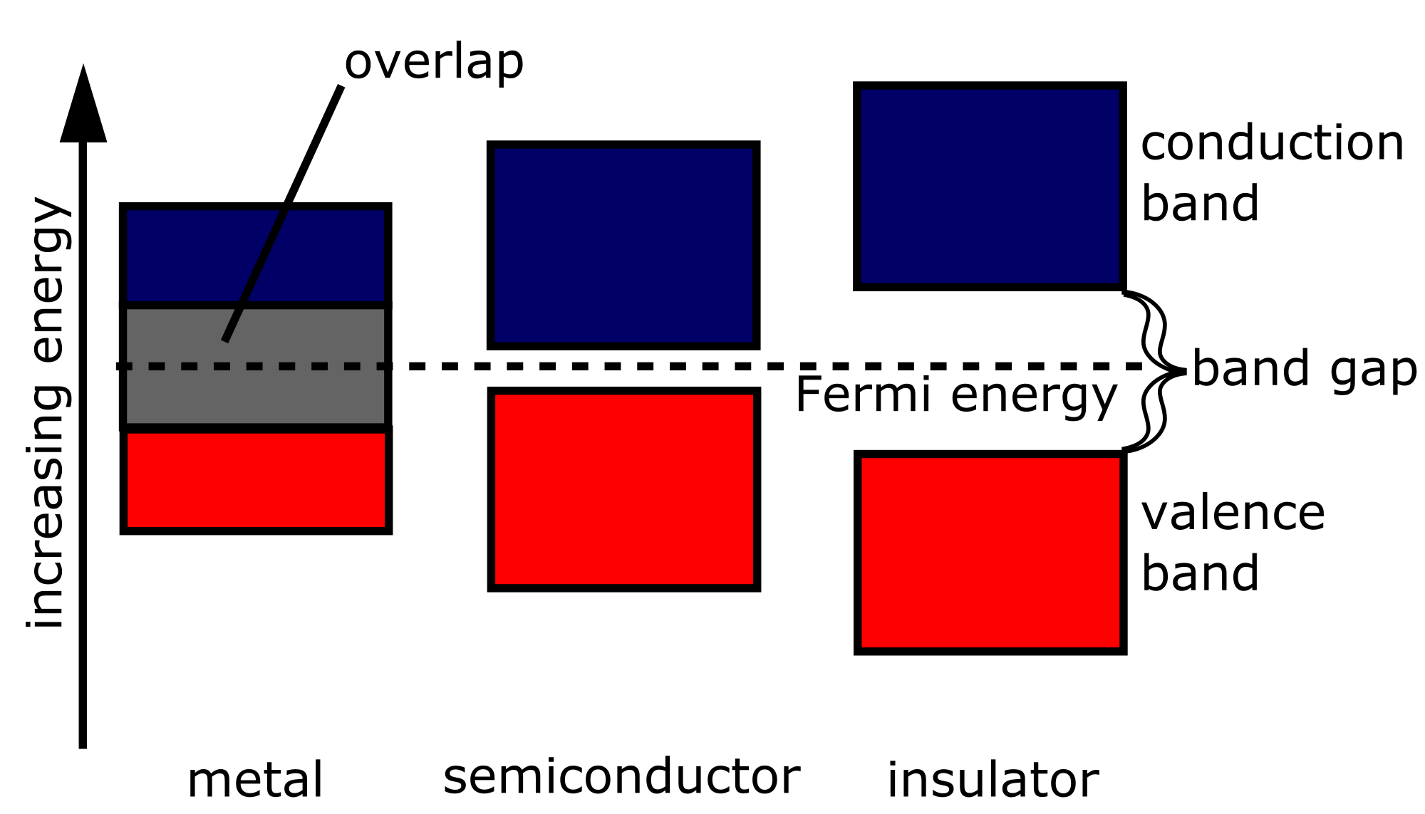
- Band gap energy difference $E_{g}$ = $E_{c}$ - $E_{v}$
- Insulators: > 5 eV
- Semiconductors: smaller gap, a small amount of electrons escape from valence band to the conduction band
- Conductors (metal, graphite): overlap (no gap)
- Direct (III+V) vs indirect (IV) band gaps
- Direct: could emit photons (LED, photo detector)
- Indirect: emit a phonon in the crystal
- The tetrahedral covalent bond crystalline structure for extrinsic (doped) semiconductors
Carriers
- Electrons (e-) in the conduction band as well as the vacancies in the valence band (holes, h+)
- For intrinsic semiconductors, motility factor $\mu$: GaN (GaAs) >Ge > Si, parallel with conductivity
- Enriched by doping (increase both $\mu$ and conductivity): making extrinsic semiconductors
- Doping group V elements (donor impurities): electrons are major carriers (N-type)
- Doping group III elements (acceptor impurities): holes are major carriers (P-type)
- N-type semiconductors have higher $\mu$ than P-type since electrons have lower effective mass than holes. Thus, N-type is better for high-freq applications. But P-type has dual role, being both resistors and semiconductor switches.
P-N junctions and diodes
Depletion zone
- Diffusion of major carriers generate an electric field across the boundary
- A zone with little carriers, high resistance
- Process a barrier voltage
Applying voltage
- Forward bias: shrinking depletion zone, high conductivity
- Reverse bias: widening depletion zone, very low conductivity (essentially open circuit until breakdown)
Shockley equation
$I_{D} = I_{S} (exp(V/V_{T}) - 1)$,
where $V_{T} = \frac{kT}{q} = \frac{RT}{F} = 26mV$ (Thermal voltage)
- Forward bias: shrinking depletion zone
- Reverse bias: widening depletion zone, very low conductivity (essentially open circuit until breakdown)
Three representations of diodes
Assuming there are internal resistance ($R_D$), threshold voltage ($V_D$).
- For $V \le V_D$, open circuit.
- For $V \geq V_D$, equivalent to a reverse voltage source of $V_D$.
- Ideal diodes: $R_D = 0$, $V_D = 0$. Forward bias: short circuit. Reverse bias: open circuit.
- With barrier voltage (Si = 0.6
0.7 V; Ge = 0.20.3V): $R_D = 0$, $V_D \neq 0$. - Practical diodes: $R_D \neq 0$, $V_D \neq 0$
Diode circuits
Transform diodes into equivalent components.
Rectifiers
Only half wave rectification was covered.

Limiters (cutters)
Filters
When the load resistance is infinite (open circuit): peak detector
When the load resistance is finite: The more discharging time scale ( $\tau = RC$ ), the less ripple voltage. ( $V_r \approx \frac{V_p}{fCR}$ when $V_r \ll V_p$ )
Voltage regulator using Zener diodes
- First unplug the Zener diode and solve the voltage across it.
- Normally operates in reverse bias. ( $V_{Z}$ = 4-6 V )
- When applied voltage > $V_{Z}$: Acts as a voltage source of $V_{Z}$. Open circuit otherwise.
- When in forward bias: similar to regular diodes ( $V_{Z}$ = 0.7 V )
- When breakdown $V_{Z}$ is independent of loading resistance.
BJT
Bipolar junction transistor on Wikipedia
Current control devices.
Symbol
NPN BJT (more common)

PNP BJT (less common nowadays)

- B: Base
- C: Collector
- E: Emitter
Math
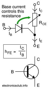
- $I_C = \beta I_B$, $\beta \gg 1$ (typically 80-180)
- $I_E = I_C + I_B = (1 + \beta) I_B$
- BArrier voltage: $V_{BE} \approx 0.7$ Volt for Si BJT. 1.1 V for GaN BJT.
- $I_{Csat} \approx \frac{V_{CC}-0.2}{R_C + R_E}$
- $\beta I_B = I_C \leq I_{Csat}$
The rest is regular circuit analysis (KCL, KVL).
One could use the fact that $I_B$ is very small ($\mu A$) compared to other currents ($mA$).
MOSFET
Voltage control devices.
- Gate voltage $V_{GS}$ is greater than threshold ($V_t$): low resistance, (ideally) short circuit.
- Otherwise, high resistance, (ideally) open circuit.